How do flex PCBs accommodate for tensile stresses?
flex PCBs accommodate for tensile stresses
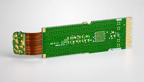
Flex PCBs have the unique ability to bend and twist, enabling them to be used in challenging application areas that would otherwise require rigid or fixed-position printed circuit boards. However, a flex PCB’s design must carefully consider how many times and to what extent it will be bent in its actual application to ensure that the board remains stable throughout the lifetime of the product.
The main concern is accommodating for tensile stresses, particularly in the transition regions between the flexible and rigid sections of the board. For example, a signal trace that runs over/under/between a mesh layer in the flex section needs to continue into the rigid section too. This is important because the mesh layer helps to maintain a controlled impedance geometry for that trace, and it’s essential not to lose that control as the board bends and twists.
It’s also important to ensure that the traces are routed in a way that minimises stress on the flex pcb section. For example, the width of a trace must be kept to a minimum where it crosses a stiffener in order to avoid a stress concentration point that could eventually lead to failure. Also, a good practice is to use curve traces wherever possible to minimize the distance over which they must be bent. This reduces the bending forces and helps to avoid cracking or breaking during a bending cycle.
How do flex PCBs accommodate for tensile stresses?
In addition, selecting the right materials is critical in both the flex and rigid sections of a flex PCB. Different materials have varying thermal expansion coefficients, which can cause reliability issues during temperature changes. The material selection is particularly crucial for the flex-to-rigid transition zones, which can be subject to very high tensile stresses.
Another key aspect of a flex PCB is the inclusion of stiffeners, which are selected areas in which rigid material is laminated to the flex circuit. The most common choice is polyimide, which is a tough material that can resist repeated creasing and movements without fatigue cracking and is extremely tolerant to the alternating expansion and contraction caused by temperature fluctuations.
Stiffeners are used to support the flex circuit in its dynamic bend region, and they should be placed in such a way that they will not interfere with plated through holes (PTHs) in the flex area or with solder paste squeegeeing or pick-and-place assembly. Stiffeners should also be designed in a way that they do not compromise the flex-to-rigid zone’s conductive properties or structural integrity.
The most important thing to keep in mind is that a flex-to-rigid zone is a high stress region of the circuit board, and the underlying materials must be designed accordingly. Careful consideration should be given to the layer stackup, as well as to the thickness and dielectrics of each material in order to achieve a balanced and robust construction. The best way to do this is to work closely with the flex PCB manufacturer early in the design process so that they can help you with your material call-outs and stack-up configurations.